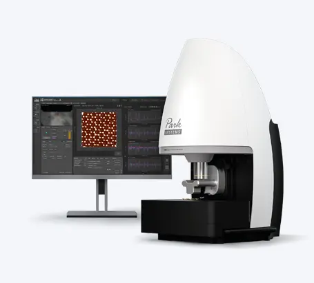


Park Systems, world leading manufacturer of Atomic Force Microscopes announced the launch of Park NX-Hybrid WLI, the first fully integrated system that combines Atomic Force Microscope (AFM) with White Light Interferometer (WLI) profilometry. White light interferometry (WLI) is a nondestructive, non-contact, optical technique used to generate 2D and 3D models of surfaces now widely used for semiconductor production quality assurance. Park Systems introduces the Park NX-Hybrid WLI as a powerful semiconductor metrology tool that incorporates the best of AFM and WLI technologies into one seamless system.
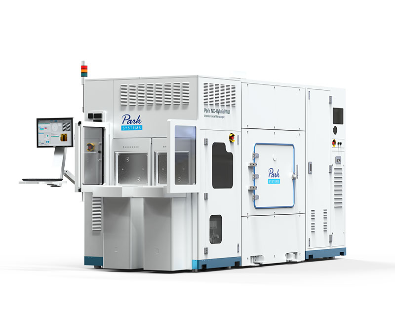
Park NX-Hybrid WLI, the first fully integrated system that combines Atomic Force Microscopy (AFM) with White Light Interferometer (WLI) profilometry, a powerful semiconductor metrology tool that incorporates the best of AFM and WLI technologies into one seamless system.
"Park NX-Hybrid WLI introduces a total complementary metrology solution for semiconductor applications requiring both large area scanning and nanoscale metrology," comments Dr. Ryan Yoo, Executive VP, Business Development, Park Systems. "The revolutionary design and seamless integration of WLI and AFM emphasizes Park's commitment to provide customer driven solutions, as nano metrology requirements for device manufacturers continues to increase."
The Park AFM in the integrated system is based on Park NX-Wafer, the industry leading automated atomic force microscopy system for semiconductor and related devices, manufacturing in-line quality assurance and research and development. The combined AFM/WLI system provides high throughput imaging over a very large area with the WLI module, and nanoscale metrology with sub-angstrom height resolution over the areas of interest using AFM. Defects of a patterned structure can be detected by comparing images of reference and target sample areas using high speed "hot spot detection", a technique enabled by fast localization for defect sites for high resolution AFM review.
The Park WLI module supports both White Light Interferometry (WLI) and Phase Shifting Interferometry (PSI) modes. The PSI mode is enabled with a motorized filter changer and the two objective lenses can be replaced automatically by the motorized lens and supports objective lens magnification of 2.5x, 10x, 20x, 50x and features a 100x CMOS camera.
Fusing two complementary techniques, Park NX-Hybrid WLI is a comprehensive automated metrology system, providing substantial cost savings over two separate systems.
"Unlike legacy standalone WLI and AFM systems, Park NX-Hybrid WLI accomplishes more, in a seamless manner, at drastically lower cost of ownership, creating a completely holistic integrated tool," comments Dr. Stefan Kaemmer, General Manager for Park Americas. "With both tools on the same mount and fed by one EFEM, the system creates fully integrated and exchangeable data, reducing the 'fab footprint' and increasing throughput over a larger area."
Park NX-Hybrid WLI was developed for use in applications requiring much higher resolution and accuracy beyond the capability of WLI alone, such as advanced chemical mechanical polishing (CMP) metrology and monitoring, dishing, erosion, and edge-over-erosion (EOE), film thickness, pillar height, hole structure and die to die comparison. It will also be useful in advanced packaging applications including through-silicon via (TSV) and micro bump measurement redistributed layer (RDL) measurement and photo resist residue detection.
The new Park NX-Hybrid is part of a series of hybrid metrology products Park Systems plans to offer this year to enhance and improve the utilization of atomic force microscopy across a wide range of industrial and academic research applications.
For more information, please visit www.parksystems.cn/hybrid-wli
About Park Systems
Park Systems is the fastest growing and world-leading manufacturer of atomic force microscopy (AFM) systems, with a complete range of products for researchers and engineers in the chemistry, materials, physics, life sciences, semiconductor and data storage industries. Our mission is to enable nanoscale advances for scientists and engineers solving the world's most pressing problems and pushing the boundaries of scientific discoveries and engineering innovations. Customers of Park Systems include most of the world's top 20 largest semiconductor companies and national research universities in Asia, Europe and the Americas. Park Systems is a publicly traded corporation on the Korea Stock Exchange (KOSDAQ) with corporate headquarters in Suwon, Korea, and regional headquarters in Santa Clara, California, USA, Mannheim, Germany, Paris France, Beijing, China, Tokyo, Japan, Singapore, India, and Mexico City, Mexico. To learn more about Park Systems, please visit www.parksystems.com.