


 Performing nanoscale measurements in high vacuum significantly improves the sensitivity and resolution of the acquired data and enhances the material analysis. Because high vacuum scanning offers greater accuracy and better repeatability than ambient or dry N2 conditions, users can measure a wide range of dopant concentration and signal response in semiconductor materials and failure analysis applications.
Learn more about advanced capabilities for nanoscale AFM characterization in high vacuum in our “Better in Vacuum” webinar series, the latest application notes, exciting scientific results from renowned research users, and more!
WEBINARS

Thursday, July 9: Advanced high vacuum Magnetic Force Microscopy (MFM): study of topological spin textures
In this webinar, Dr. Karim Bouzehouane, CNRS Thales France, presents the capabilities of Magnetic Force Microscopy #MFM in high vacuum for studying of topological spin textures.
Register here.

Thursday, 23 July: Better in Vacuum – how high vacuum improves the accuracy of nanoscale AFM characterization (on NX-Hivac AFM)
The webinar will give a full introduction to the high vacuum AFM functions and will show the easy-to-use pumping station interface. Moreover, some test measurements will be performed in Frequency Modulation AFM.
Register here.
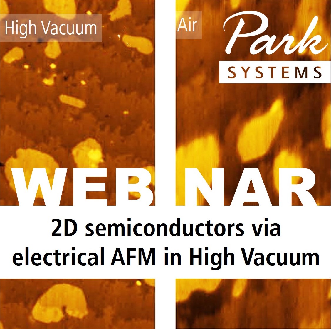
Thursday, 3 September: Better in Vacuum – boosting the characterization of 2D semiconductors via electrical AFM in high vacuum
Register here.
APPLICATION NOTES
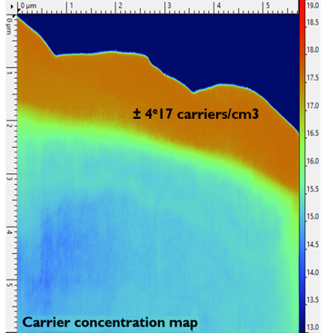
Pushing the sub 10 nm nodes device characterization with high vacuum SSRM providing the highest spatial resolution and high vacuum SCM improving carrier type sensitivity.
Read the app note: Carrier profiling in high vacuum using Scanning Spreading Resistance Microscopy and Scanning Capacitance Microscopy
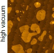
Investigating 2D materials: the advantages of high vacuum for electrical measurements utilizing the capabilities of the Park NX-Hivac atomic AFM using MoS2 as an example material.
Read the app note: Advantages of high vacuum for Electrical Scanning Probe Microscopy
Understanding the electrical and mechanical properties of Lithium ion batteries (LIBs) for modern battery applications by using PinPoint™ Scanning Spreading Resistance Microscopy
Read the app note: Electrical and Mechanical Characterization of Li Ion Battery Electrode using Pinpoint SSRM
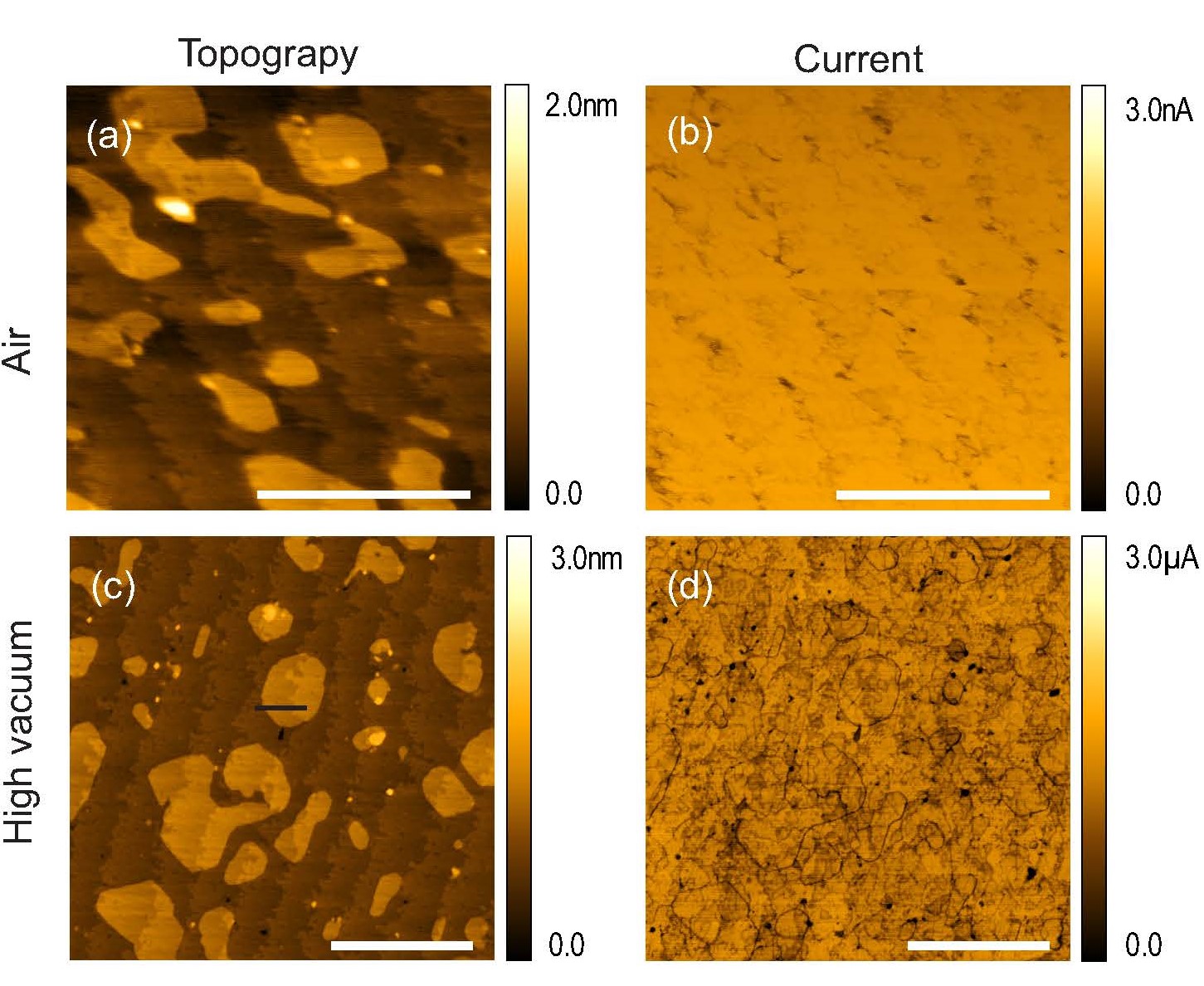
Performing scanning spreading resistance microscopy (SSRM) and conductive AFM (C-AFM) in high vacuum significantly improves accuracy, repeatability and homogeneity of data.
Read the technical note: Better in Vacuum: on the advantages of High Vacuum environment for Electrical Atomic Force Microscopy
PUBLICATIONS
Nanoscale Localization of an Atom Probe Tip through Electric Field Mapping I Read the paper
In this paper researchers propose a novel method to measure atom probe tomography (APT) specimen in three dimensions without damaging the SPM probe or specimen. The Electrostatic Force Microscopy (EFM), performed on Park NX-Hivac #AFM, is free of any mechanical interaction between both tips prior to surface imaging and is applicable for all possible probe geometries. The study is promising for further development of experimentally probing the 3D electric field distribution around an APT tip.
INTERVIEW
Rising Star of High Vacuum AFM and the AFM Scholarship Winner, Dr. Yuanyuan Shi

Dr. Yuanyuan Shi is a Postdoctoral fellow (Funded by Marie Curie Fellowship from European Commission) at IMEC, Belgium. Her expertise spans the development of wafer-scale two-dimensional (2D) materials based on transistor technology for scaling high-performance logic devices beyond 3 nm technology node.
Dr. Shi published over 50 scientific papers, she is an active reviewer for i.a. Nature, Nature Electronics, IEEE Electron Device Letters, and she is a member in IEEE EDS Nanotechnology committee. She has been recognized as a Forbes 30 under 30 (one of the world’s most impactful community of young entrepreneurs and game-changers) in 2020 and also as one of the Rising Stars Women in Engineering in 2018.
What is the impact of your research:“We are making efforts to achieve wafer-scale, uniform and single-crystalline growth of 2D materials, wafer-scale and clean transfer of 2D materials, and improvements to solve the specific issues (contact resistance, gate stacks, variability, reliability, yield, etc.) for large-area integration of 2D materials based nanoelectronics. Our research work will pave the way to large-area integration and industrialization of 2D materials-based transistors for beyond 3 nm technology node.”
Read the full interview.