


Advanced Vector Nanolithography Using Closed Loop Scan System
Nanolithography
Normally, AFM is used to image a surface without damaging it. However, AFM can be used to modify the surface deliberately by applying either excessive force or high-field pulses. Scientific literature as well as newspapers and magazines have all shown examples of surfaces that have been modified atom by atom. This technique is known as Nanolithography.
Nanolithography patterns are created on the sample surface by two methods as shown in Figure 1. The first method is to scratch the sample surface with hard tips, mechanically deforming the sample surface. The second method is to apply a bias between the tip and the surface, inducing a change of the surface's chemical properties. The lithographic patterns can be generated in diverse forms: point or grid. Raster Nanolithography is common where the entire image is scanned.
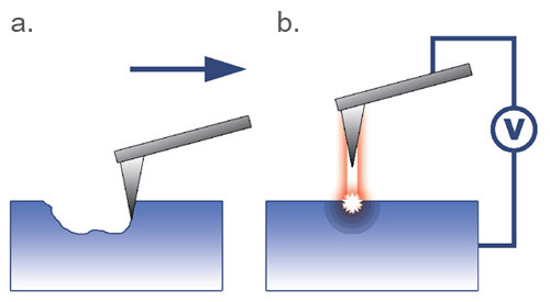
Figure 1. Pattern created on the surface by plowing the surface with the tip (a) and by changing the surface with applied bias (b).
Vector Nanolithography Means Advanced Closed Loop Scan System
When it comes to Nanolithography, the value of an advanced closed-loop system cannot be emphasized enough. It is no exaggeration that the reliability and efficiency of Nanolithography depends on it. With a state-of-the-art closed-loop system offered by with Park AFM, vector Nanolithography can be realized.
Park AFM uses a Position Sensitive Photo Detector (PSPD) in the XY-scanner as the closed loop sensor. This PSPD monitors the movement of XY-scanner and controls it in real-time. Doing so enables the vector movement of the cantilever in the XY direction. In other words, rasterization, a common method used in Nanolithography of other AFM systems, is not necessary for Park AFM (although it is provided with the system). In a way, vector Nanolithography is the ultimate measure of a closed-loop system's performance.
From Figure 2, the advanced performance of vector nanolithography is demonstrated. The Nanolithography image in Figure 2 (b) was written with two circles and two lines, individually in vector as shown in Figure 2 (a). The width of lines depends on several factors such as the applied voltage and/or the atmosphere humidity during the scan. Note that there is no distortion of the image even though the lines were drawn in vector movement, not raster.
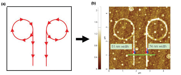
Figure 2. Vector Nanolithography. The image is generated in vector by applying negative voltage between -5 and -10 V. Scanning rate was varied between 1 and 0.1 μm/s. The height of deposited oxide is about 2-4 nm.
XEL - Advanced Nanolithography Software
Nanolithography processes of the Park AFM are controlled by XEL lithography software. XEL has a convenient user interface which makes the lithography process as easy as drawing a picture with simple graphics software. Just by simple mouse manipulation, objects can be easily drawn in the software, resized, and moved before they are translated onto the sample surface. Bitmap images can be imported for raster and vector Nanolithography respectively.
The XEL software has the following advantages:
• A variety of lithography modes
• Separates Background and Object properties.
• Supports both Vector mode and Raster mode
• Provides a convenient Graphic Editor
Figure 3 is a bitmap image pattern generation using voltage-induced Si oxidation. The electrical domain of PZT film can be switched by applying different biases between the tip and sample at different positions. Figure 4 shows (a) before and (b) after the domain switching of the EFM images of a PZT film. Light colored regions are biased by 10 V and dark regions are biased by -10 V.
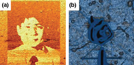 Figure 3. Bitmap image pattern generation using (a)domain switching on PZT film, and (b) nanoscratch on polycarbonate film, 30 μm scan size.
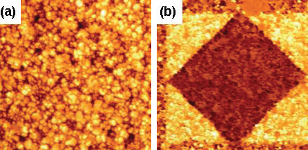
Figure 4. EFM image of lithography performed on PZT film (a) before and (b) after the domain switching, 5 μm scan size.
External High Voltage Lithography
Nanolithography of Park AFM is a technique used to pattern nanoscale shapes on the sample surface. For ordinary Nanolithography mode using the Park AFM, the available range of the applied voltage is -10 V to +10 V. For special situations requiring a higher voltage range, High Voltage Nanolithography mode has been developed. With the External High Voltage toolkit, Park AFM can be connected to an external voltage amplifier enabling experiments or measurements with tip or sample biases exceeding 10 V. The available voltage range for High Voltage Lithography depends on the external voltage amplifier.
Applications:
• Develop NanoLithographic media and techniques
• Study minimum feature size
• Minimum line spacing
• Resist exposure speed
• Exposure threshold