


High Spatial and Thermal Resolution Microscopy by the Park AFM Innovations
High Resolution Scanning Thermal Microscopy (SThM) with the Park AFM Series
There has been growing interest in the heat dispersion of nanostructured materials. Park AFM's Scanning Thermal Microscopy (SThM) mode was developed to probe thermal properties at the nanoscale level. SThM uses nanofabricated thermal probes with resistive elements to achieve unprecedented high spatial and thermal resolution and sensitivity with a unique signal detection scheme. SThM with Park AFM is available in two modes: Temperature Contrast Microscopy (TCM) and Conductivity Contrast Microscopy (CCM). TCM allows the user to measure the temperature variations on a sample surface. CCM allows the user to measure variations of thermal conductivity on a sample surface.
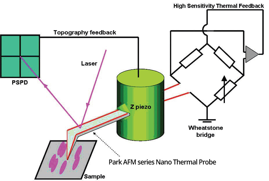
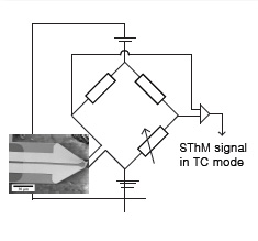
Figure 1. Schematic diagram of the series SThM system
Figure 1 shows the schematic diagram of system behind SThM with Park AFM. A "V" shaped resistive element is mounted at the end of a cantilever. While the distance between the probe tip and sample surface is controlled by a usual AFM scheme, The thermal probe forms one leg of a Wheatstone bridge (Figure 1). It is this Wheatstone bridge which feedbacks, adjusts, and balances the bridge voltage in order to measure the probe's temperature (in TCM) or maintain a constant probe temperature (in CCM). A topographical AFM image can be generated from changes in the cantilever's amplitude deflection. Thus, topographic information can be separated from local variations in the sample's thermal properties, and the two types of images can be collected simultaneously.
Park AFM's Nano Thermal Probe
The key part of the SThM is the SThM tip, which serves as a resistance thermometer (or a heater in CCM mode) at the same time as it acts as an AFM tip. The resistivity of the SThM tip is changed according to the temperature of the surface in contact and is read from the Wheatstone bridge. Previous SThM designs, which were made by etching a wire, could not provide sufficient spatial and thermal resolution, critically limited by the geometry of a wire-based thermal probe (i.e., Wollastone wire). SThM with Park AFM uses a nanofabricated thermal probe where a resistive element is lithographically patterned onto the AFM tip.
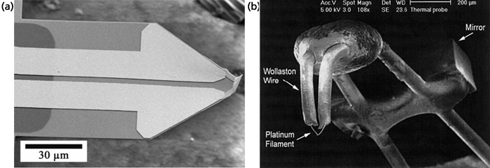
Figure 2. The SEM images of (a) a Park AFM Nano Thermal Probe and (b) a Wollaston wire.
Figure 2 (a) and (b) shows scanning electron microscopy (SEM) images of a typical Wollaston wire thermal probe and the nanofabricated thermal probe used in SThM with Park AFM. The tip radius of the nanofabricated probe is about 100 nm enabling high resolution thermal image scan while a Wollaston wire probe's tip radius is over several hundred nm.
|
|
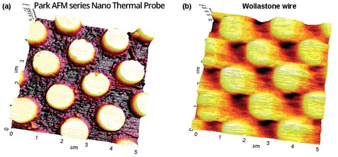
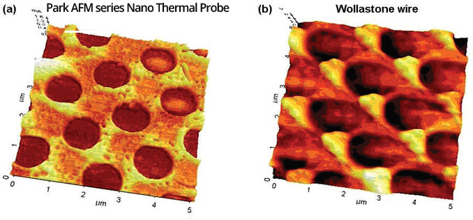
| Figure 3. Topography image comparison of HSQ posts of 1 μm diameter patterned on a silicon substrate (5 µm scan size) using (a) Park AFM series Nano Thermal Probe and (b) Wollastone wire. | Figure 4.Thermal conductivity image comparison of HSQ posts of 1 μm diameter patternedon a silicon substrate (5 µm scan size) using (a) Park AFM series Nano ThermalProbe and |
In Figure 3 and 4, a comparison is made between the performance of a Park Nano Thermal Probe and a Wollastone wire probe. The imaged sample is a set of hydrogen silsesquioxane (HSQ) posts each with 1 µm diameters on a silicon substrate. The detailed differences in topographic and thermal conductivity resolution are clearly demonstrated with the Park Nano Thermal Probe which has superior spatial and thermal resolution. Please note that such dramatic enhancements in resolution and sensitivity are realized only by combining the advantages of the nanofabricated thermal probe and the SThM mode sensitivity offered by the Park AFM.
Temperature Contrast Mode (TCM)
In TCM mode, the resistive element of the Park Nano Thermal Probe is used as a resistance thermometer. The temperature of the thermal probe changes as the tip scans the surface according to the surface temperature. Change of the wire temperature leads to change of its resistance. The temperature of a very small region can be measured by running a constant current, referred to as the 'Probe Current,' through the probe and measuring the resistance as shown in Figure 5. First, the tip is put into thermal equilibrium with the sample surface and thus its resistance is constant. At this time, the variable resistor in the bridge is adjusted so that the potential difference between its two points becomes zero. Then, the temperature of the probe changes as the probe scans over the surface. The corresponding change in probe resistance will alter the voltage balance of the bridge, changing the voltage difference between the bridge's two points. This is referred to as 'SThM error'. This SThM error is used to generate the SThM image in TCM mode.
The current passed through the probe in TCM is set to be small enough that no self-heating of the probe occurs. Resistance change due to the self-heating would cause errors in temperature measurement. Also, the scanning speed in TCM mode is limited by the time it takes for the tip to reach thermal equilibrium with the sample surface.
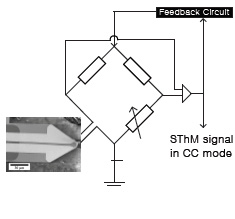
Conductivity Contrast Mode (CCM)
In Conductivity Contrast Mode, (CCM) the resistive element of the Park Nano Thermal Probe is used as a resistive heater. Sufficient energy is applied to the probe tip to keep it at a set temperature via a feedback loop. The energy required to maintain the set temperature represents the local thermal conductivity. Schematic diagram of the CCM is shown in Figure 6.
When the heated probe, preset at a value much higher than a sample temperature, makes contact with the sample, heat flows from the probe to the sample which results in the cooling of the probe. The feedback senses this shift, balances the bridge voltage, and restores the probe's resistance (or temperature) to its preset value. The raw data from the SThM with Park AFM reflects the feedback voltage, Vout, applied to the bridge.
The heat flow between tip and specimen under investigation is controlled by the following three factors:
• Thermal conductivity of the sample
• Contact area of the probe
• Temperature difference of the probe and the sample
|
|
|
Figure 5. Schematic diagram of the TCM mode. |
Figure 6. Schematic diagram of the CCM mode. |
For most samples, changes in the probe-sample contact area are negligible and, due to its large thermal mass, the sample remains at a constant temperature. The temperature difference between the probe tip and the sample also stays constant since the temperature of the probe is controlled by the feedback loop. As a result, the changes in heat flow will be only caused by changes in thermal conductivity of the sample.
As the thermal conductivity of the sample varies during the scan, the probe's temperature tends to change. However, the Wheatstone bridge uses the SThM error and feedback loop to balance the voltage applied to the tip in order to maintain its temperature constant at the preset value.
Nanoscaled Thermal Imaging by the Park AFM
Figure 7 shows the high resolution topography and thermal conductivity image of a 4.3 μm diameter HSQ post on a silicon substrate as acquired the Park Nano Thermal Probe. Inhomogeneity in the thermal conductivity, due to impurities in the HSQ's composition, is observed in contrast to a flat topography.
In Figure 8, the high resolution topography and thermal conductivity of smaller HSQ posts with 0.2 μm diameter on a silicon substrate are imaged, again, using the Park Nano Thermal Probe. In the thermal conductivity image, one can also observe the impurities which are not apparent in the topography image.
It is evident that SThM with Park AFM's has superior spatial and thermal resolution. It opens up great possibilities in the nanoscale investigation of thermal properties in various nanostructured materials.
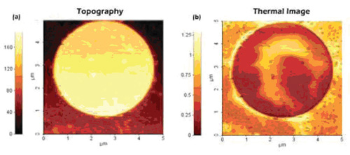 Figure 7. (a) High resolution SThM topography and (b) thermal conductivity image of a HSQ post with 4.3 μm diameter on a silicon substrate (5 µm scan size) by the Park AFM's SThM with Nano Thermal Probe.
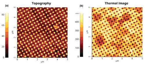
Figure 8. (a) High resolution SThM topography and (b) thermal conductivity image of HSQ posts with 0.2 μm diameter on a silicon substrate 5 µm scan size) by the Park AFM's SThM with Nano Thermal Probe.