


John Paul Pineda, Charles Kim, and Byong Kim
Park Systems, Inc., Santa Clara, CA USA
Introduction
Sophisticated, high-performing technology often requires electrical components with advanced material properties [1]. For example, TiO2 thin film, a versatile compound, is widely used as a charge selective transport layer in solar cells and as a high capacity anode for Li-Ion batteries. For battery applications, this material exhibits superior cycling stability and Coulombic efficiency compared to other transition oxides [2]. Another functional material used in advanced technology components is SiC, which is applied in power devices to improve dielectric breakdown field strength, bandgap, and thermal conductivity [3]. For the battery and semiconductor industries to conduct nanoscale electrical measurements during manufacturing, an innovative and precise nanoscale characterization technique for electrical analysis is required.
Conductive Atomic Force Microscopy (C-AFM) and Scanning Spreading Resistance Microscopy (SSRM) are effective techniques for studying electrical properties of advanced materials. These techniques measure electrical properties by monitoring the current flowing between the conductive tip and the sample during topography measurements. Sensitivity in these techniques can be further improved by controlling the measurement environment. A previous study shows that using C-AFM in a vacuum environment eliminates the layer of contaminants (water and hydrocarbons) that form on the tip, and prevents oxidation during scanning, allowing for a longer tip lifetime and better sensitivity [4, 5]. In this technical note, a study of two different samples with the Park NX-Hivac atomic force microscope demonstrates the advantage of a high vacuum environment for C-AFM and SSRM measurements. The results show improved sensitivity and resolution in the measurements under high vacuum conditions when compared to ambient air.
Experimental
Two samples are selected and investigated using a Park NX-Hivac system. The first sample is a Silicon Carbide (SiC) MOSFET and the second sample is a TiO2 thin film deposited on a Au/Ti/SiO2 substrate, hereafter referred to as Sample 1 and Sample 2, respectively. Images for Sample 1 are acquired in SSRM Mode using a scan rate of 0.5 Hz and a scan size of 1.5 µm x 1.5 µm. Images for Sample 2 are acquired in C-AFM Mode with a scan rate of 1.0 Hz and a scan size of 1.5 µm x 1.5 µm. In SSRM imaging, a full diamond tip CAMS FDP (nominal spring constant k = 27 N/m) is used, while a CDT-Contr (nominal spring constant k = 0.5 N/m) is used in C-AFM. A silver paste is applied on top of the sample, as well as on the metal sample holder under the sample to ensure electrical connection from the bias line. The samples are measured under ambient air and vacuum (in the low 10-5 Torr range) conditions to understand the influence of the environment on C-AFM and SSRM measurements.
C-AFM and SSRM operate in the Contact mode regime, and their imaging principles are relatively similar. When DC bias is applied, the current flow between the conductive tip and sample is monitored, and the electrical properties are measured. The conductive tip acts as an electrode. Generally, the current has a very low magnitude; therefore, a current amplifier is needed to amplify the current signal. The current amplifier both increases and monitors the current, which is then processed into an image. In this experiment, the applied DC bias is +2.5 V for Sample 1 and +4 V for Sample 2. The main differences between the two techniques are their applications, and the type of current amplifiers needed. C-AFM is commonly used for current variations mapping, while SSRM measures the local resistance and conductance of a surface. The SSRM mode of Park Systems uses a logarithmic current amplifier to measure a wide range of resistance distribution in a small area. In contrast, C-AFM mode uses a linear current amplifier.
Figure 1 shows a schematic view of a C-AFM and SSRM set-up on the Park NX-Hivac system. The AFM cantilever tip, coated with a conductive material, connects to a current amplifier and can thus measure a wide range of current signal. The current amplifier measures the electric current flow at the tip-sample contact point. As in other AFM modes, the super luminescent diode (SLD) light beam and position sensitive photodiode (PSPD) serve as feedback (Feedback Control) to detect topographic features. The AFM controller then measures and processes these changes to obtain the topography and electrical current C-AFM or SSRM image.
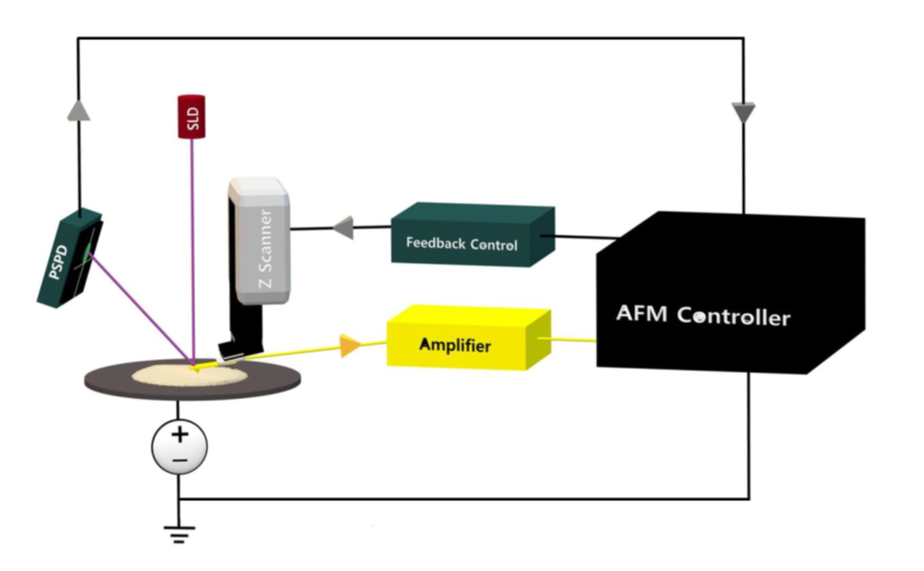
Figure 1. Schematic Illustration of C-AFM and SSRM AFM.
Results and Discussion
Figure 2 presents topography and resistance images of Sample 1 obtained in ambient air and high vacuum using SSRM mode. The topography images in Figures 2a and 2b show a polished surface with a height difference of 109 nm on the cross-section. However, they do not contain significant information related to the device pattern. The measurement positions in both images are the same in ambient air and in high vacuum, as can be seen in their matching topography line profiles in Figure 2c. Therefore, environmental comparison is possible. Figures 2d and 2e are the resistance images taken simultaneously with the topography images in Figures 2a and 2b, respectively. By Figures 2d and 2e, the resistance image taken in high vacuum shows more features and details than the one taken in air. In fact, line profiles of the resistance images, as shown in Figure 2f, show a significant difference in the resistance distribution in air and vacuum. Since there is no oxidation or water layer in the vacuum, the SSRM shows a higher sensitivity in a vacuum than in air due to the improved electrical contact between the tip and sample. Characterizing electrical properties with this level of detail is essential for understanding the functionality of a MOSFET device.

Figure 2. Topography and resistance images measured on a SiC MOSFET sample in ambient air and high vacuum using SSRM mode. (a) Topography in air (b) and vacuum (c) and the corresponding line profiles. (d) Resistance image in air (e) and vacuum (f) and the corresponding line profiles.
Figure 3 presents the current images of Sample 2 obtained in ambient air and high vacuum using C-AFM mode. Small grain-structures with distinct contrast are visible in the current image obtained in high vacuum, while the current image in air shows less detail. The maximum current measured in high vacuum is 827 nA, while it is 59 nA in air. The line profiles of the current images, as shown in Figure 3c, confirm that a consistently larger current is measured in high vacuum than in air. This improved electrical sensitivity in high vacuum is likely due to the removal of water and contaminants that are typically present on the sample surface in air.
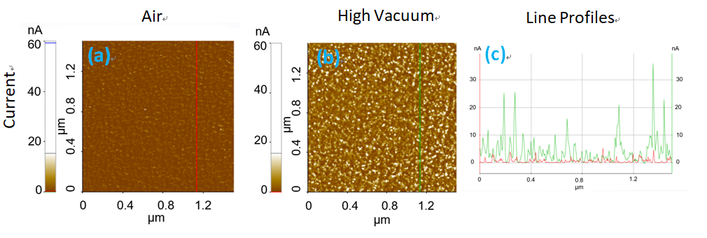
Figure 3. Current images measured in TiO2/Au/Ti/SiO2 sample in ambient air and high vacuum using C-AFM mode. (a) Current image in air (b) and vacuum (c) and the corresponding line profiles.
Conclusion
This application note examines the current image quality of the SSRM and C-AFM modes of the Park NX-Hivac atomic force microscopy system. Two samples, a SiC MOSFET and a TiO2/Au/Ti/SiO2, are tested under ambient air and high vacuum conditions to study the sensitivity of electrical measurements using both modes. The results show that in high-vacuum environments, the sensitivity of the electrical characterization improves. In a high vacuum, the residues are relatively negligible, which increases the electrical contact at the tip-sample surface. Therefore, the current can pass more freely and expose the current contrast of smaller features with a higher definition. In conclusion, operating the Park NX-Hivac system in high vacuum offers detailed insights for various nanotechnology applications and allows for a better understanding and control of the electrical behavior of advanced materials and devices at the nanoscale.
References
1. Puetz, et al., Characterization of Electrical Properties. DOI: 10.1007/978-3-319-19454-7_52-1
2. M. Madian, et al., Current Advances in TiO2-Based Nanostructure Electrodes for High Performance Lithium Ion Batteries.
3. ROHM Semiconductor, SiC Power Devices and Modules Application Note. Issue of August 2014 14103EBY01
4. L. Aguilera, et al., Influence of vacuum environment on conductive atomic force microscopy measurements of advanced metal-oxide-semiconductor gate dielectrics. DOI: 10.1116/1.2958246.
5. J. Ludwig, et al., Advantages of High Vacuum for Electrical Scanning Microscopy. https://parksystems.com/images/media/appnote/App_Note_36_Advantages-of-High-Vacuum-for-Electrical-Scanning-Probe-Microscopy_correctionsIH_JS_1.pdf