


Probing the Local Electronic Structure of a Sample’s Surface
Scanning Tunneling Microscopy (STM) is one of the application modes for Park AFM. STM is the ancestor of all atomic force microscopes. It was invented in 1981 by Gerd Binnig and Heinrich Rohrer at IBM Zurich. Five years later, they were awarded the Nobel Prize in physics for its invention. The STM was the first instrument to generate real-space images of surfaces with so-called "atomic resolution." This would later be known as atomic lattice resolution.
The operation of STM and Conductive AFM is identical except that one uses a sharpened and conducting wire/tip in STM instead of a conductive AFM cantilever. A bias voltage is applied between the tip and the sample. When the tip is brought within about 10 Å of the sample, electrons from the sample begin to "tunnel" through the 10 Å gap into the tip or vice versa, depending upon the sign of the bias voltage as shown in Figure 1. The resulting tunneling current varies with tip-to-sample spacing, and both the sample and the tip must be conductors or semiconductors. Thus, STM cannot image insulating materials.
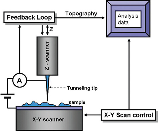
Figure 1. Schematic diagram of the Park AFM STM STM system
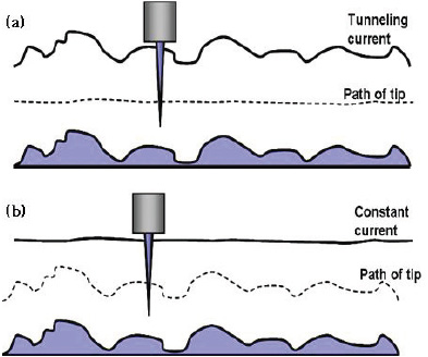
Figure 2. Comparison of (a) constant-height and (b) constant-current mode for STM.
The tunneling current is an exponential funtion of distance. Based on quantum mechanics, the tunneling current (It) is,

Here, d is the distance between tip and sample surface.
If the separation between the tip and the sample changes by 10% (on the order of 1 Å), the tunneling current also changes by an order of magnitude. This exponential dependence gives STMs their remarkable sensitivity. STMs can image the surface of the sample with sub-angstrom precision vertically and atomic resolution laterally.
STM techniques encompass many methods: taking "topographic" (constant-current) images using different bias voltages and comparing them, taking current (constant-height) images at different heights, and ramping the bias voltage with the tip positioned over a feature of interest while recording the tunneling current. The last example results in current vs. voltage (IV) curves characteristic of the electronic structure at a specific XY location on the sample surface. STMs can be set up to collect IV curves at every point in a data set, providing a three-dimensional map of electronic structure. With a lock-in amplifier, dI/dV (conductivity) or dI/dz (work function) vs. V curves can be collected directly. All of these are ways of probing the local electronic structure of a surface using an STM.
The schematics of constant-height or constant-current mode are shown in Figure 2. In constant-height mode, the tip travels in a horizontal plane above the sample and the tunneling current varies depending on topography and the local surface electronic properties of the sample. The tunneling current measured at each location on the sample surface constitute the data set, creating the topography image in Figure 2 (a).
In constant-current mode, STMs use feedback to keep the tunneling current constant by adjusting the height of the scanner at each measurement point in Figure 2 (b). For example, when the system detects an increase in tunneling current, it adjusts the voltage applied to the Z-axis scanner to increase the distance between the tip and the sample. In constant-current mode, the motion of the scanner constitutes the data set. If the system keeps the tunneling current constant to within a few percent, the tip-to-sample distance will be constant to within a few hundredths of an angstrom.
Each mode has advantages and disadvantages. Constant-height mode is faster because the system doesn't have to move the scanner up and down, but it provides useful information only for relatively smooth surfaces. Constant-current mode can measure irregular surfaces with high precision, but the measurement takes more time.
As a first approximation, an image of the tunneling current maps the topography of the sample. More accurately, the tunneling current corresponds to the electronic density of states at the surface. STMs actually sense the number of filled or unfilled electron states near the Fermi surface, within an energy range determined by the bias voltage. Rather than measuring physical topography, it measures a surface of constant tunneling probability.
From a pessimist's viewpoint, the sensitivity of STM to local electronic structure can cause trouble if you are interested in mapping topography. For example, if an area of the sample has oxidized, the tunneling current will drop precipitously when the tip digs a hole in the surface.
From an optimist's viewpoint, however, the sensitivity of STM to electronic structure can be a tremendous advantage. Other techniques for obtaining information about the electronic properties of a sample detect and average the data originating from a relatively large area, a few microns to a few millimeters across. STM can be used as a surface analysis tool that probes the electronic properties of the sample surface with atomic resolution. Figure 3 shows the (a) topography and (b) STM image of highly ordered pyrolytic graphite (HOPG).
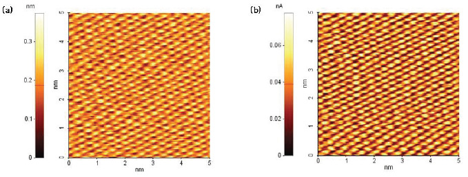
Figure 3. (a) Topography and (b) STM current image of HOPG. (5 nm scan size)
There are two current amplifiers available for STM with Park AFM: 'Internal STM' and 'External STM'. The 'Internal STM' mode refers to the STM mode that uses the fixed-gain current amplifier in the head extension module. The range of the measurable tunneling current in this mode is fixed because the gain of the amplifier is fixed. But in 'External STM' mode, measurable tunneling current range can be changed by varying the gain of the amplifier. The 'External STM' mode refers to the STM mode that uses the external low-noise current amplifier with variable gain (See "External Low Current Amplifier").
I/V spectroscopy mode supports the acquisition of current (I) vs. voltage (V) curves to investigate electrical properties of a sample surface. An I/V curve is a plot of the current as a function of the tip bias voltage applied to the sample.
Required Options
Internal
STM
STM Probes & STM Probe Holder
Head Extension module & Frame module
External
STM
STM Probes & STM Probe Holder
External Low Noise Current Amplifier
Head Extension Module & Frame Module