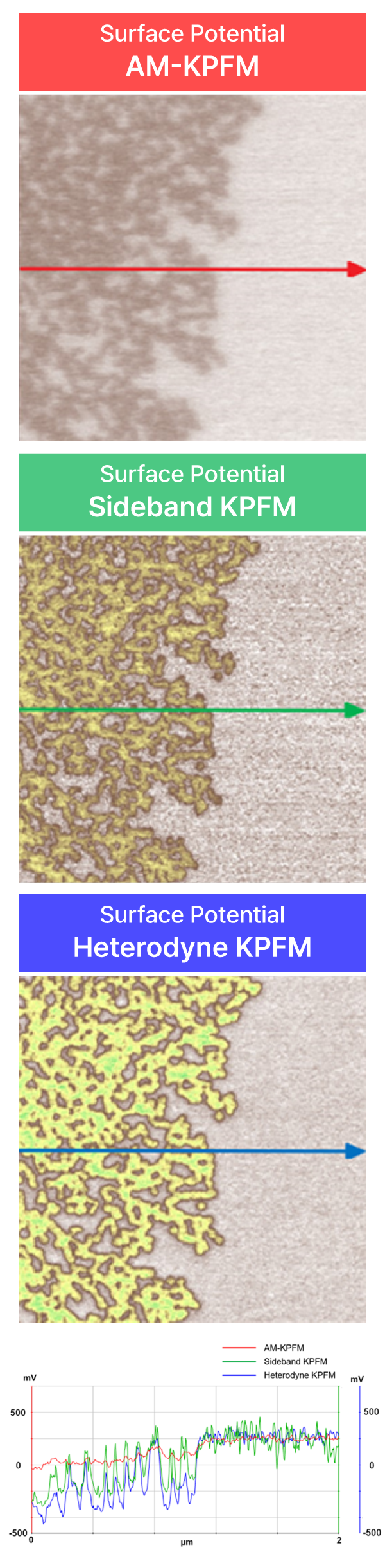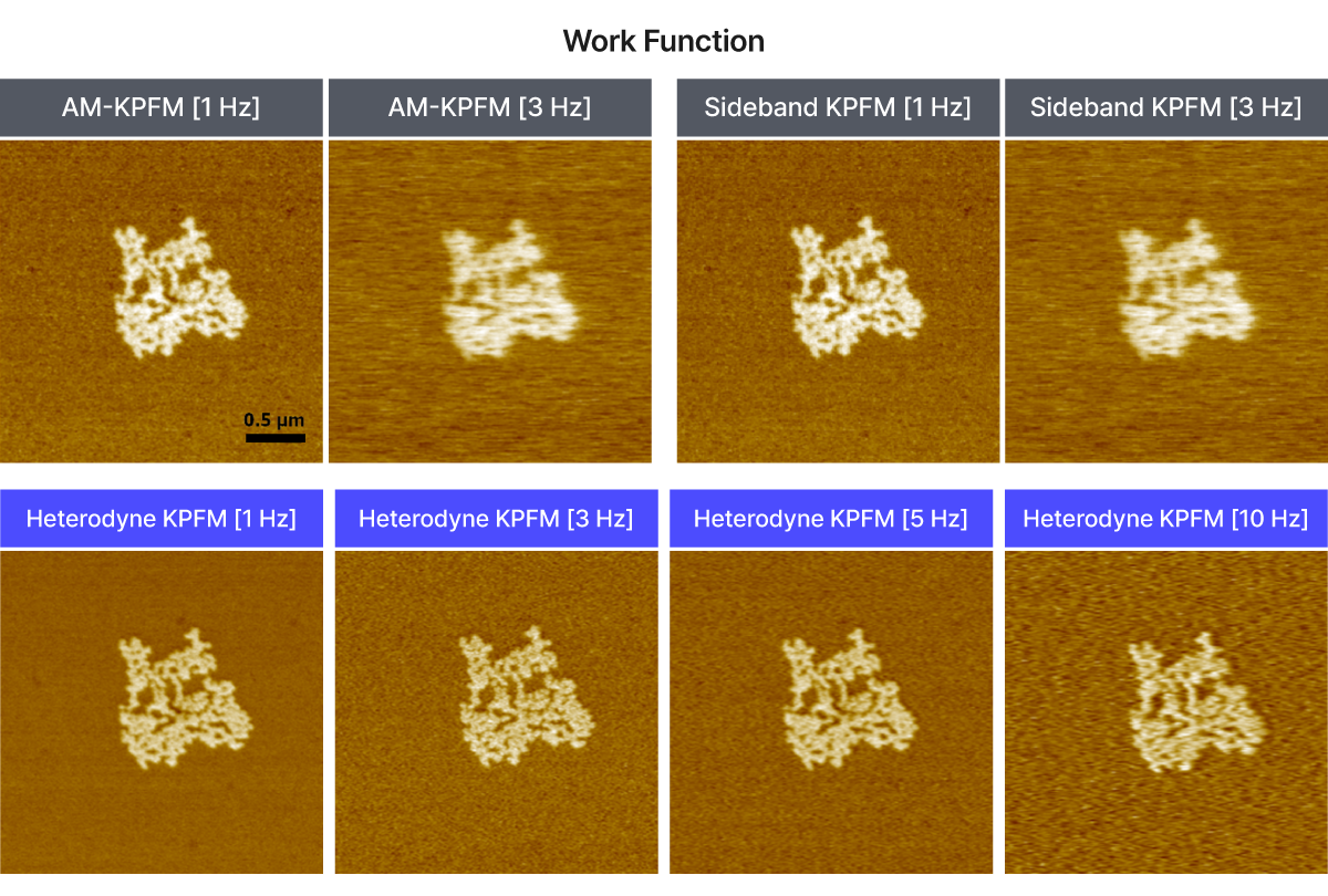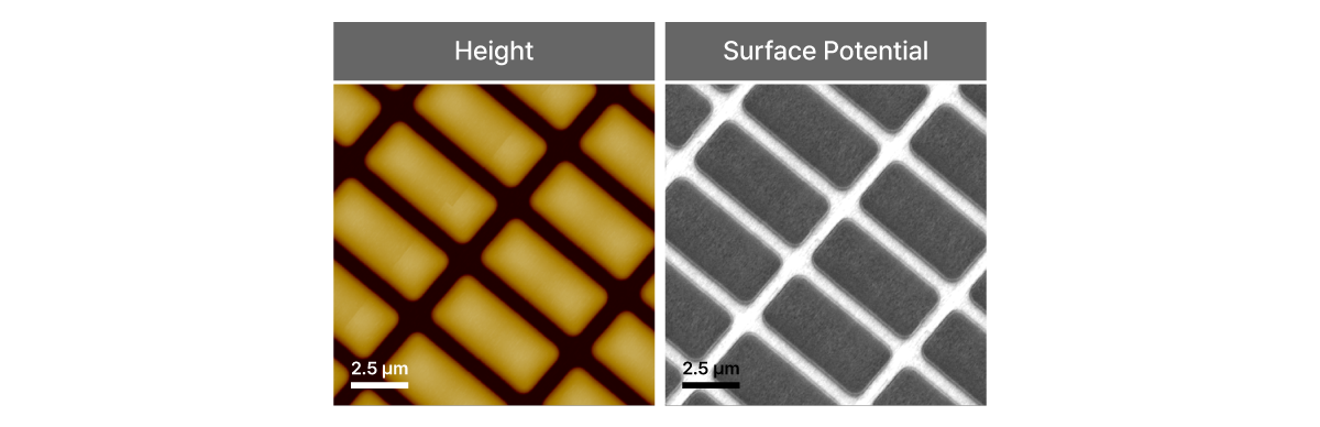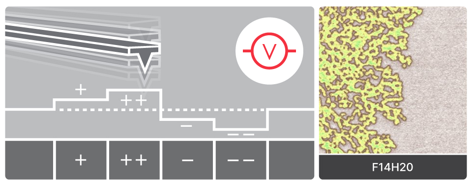
Heterodyne Kelvin Probe Force Microscopy
Heterodyne KPFM
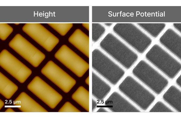
Superior surface potential detection with high spatial resolution by frequency mixing away from cantilever resonance, reducing noise and topography crosstalk