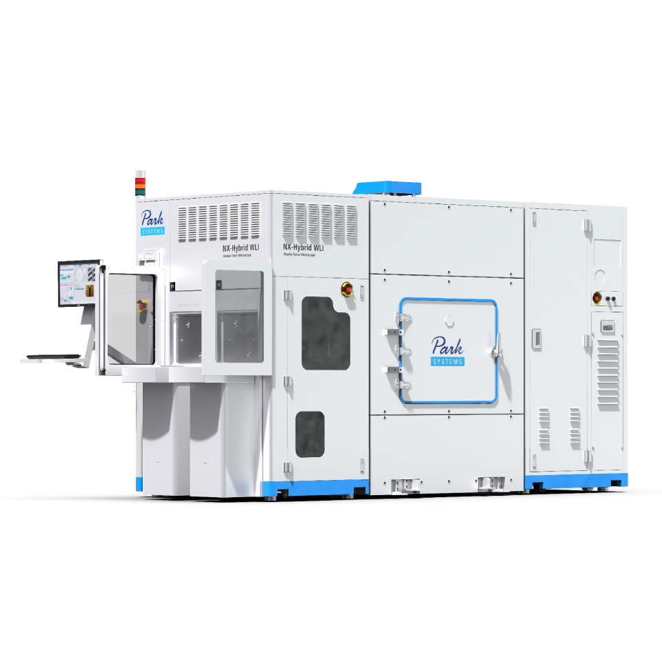
Optical profilometry enables fast, non-contact surface metrology for accurate characterization of wafer topography, thin films, and micro-scale structures across large areas. With nanometer-level vertical sensitivity and robust measurement stability, Park’s full automated optical profilometry systems provide reliable surface analysis for a wide range of semiconductor and advanced manufacturing applications.