


High Resolution and High Sensitivity Imaging of Electrostatic Force
Unique Enhanced EFM Capabilities Provided by Park AFM
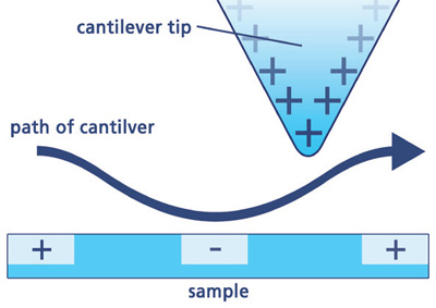
Figure 1. EFM maps locally charged domains on the sample surface.
Electrostatic Force Microscopy (EFM) with Park AFM maps electric properties on a sample surface by measuring the electrostatic force between the surface and a biased AFM cantilever. EFM applies a voltage between the tip and the sample while the cantilever hovers above the surface, not touching it. The cantilever deflects when it scans over static charges, as depicted in Figure 1.
EFM images contain information about electric properties such as the surface potential and charge distribution of a sample surface. EFM maps locally charged domains on the sample surface, similar to how Magnetic Force Microscopy plots the magnetic domains of the sample surface. The magnitude of the deflection, proportional to the charge density, can be measured with the standard beam-bounce system. Thus, EFM can be used to study the spatial variation of surface charge carrier. For instance, EFM can map the electrostatic fields of an electronic circuit as the device is turned on and off. This technique is known as "voltage probing" and is a valuable tool for testing live microprocessor chips at the sub-micron scale.
Four different EFM modes, distinguished by the method which the surface electrical information is obtained, are provided by Park AFM. These are standard EFM, Enhanced EFM, Park Systems' own patented Dynamic-Contact EFM (DC-EFM), and Scanning Kelvin Probe Microscope (KPFM). Enhanced EFM for Park AFM contains EFM (one-pass) mode, DC-EFM, and KPFM.
Principle of EFM
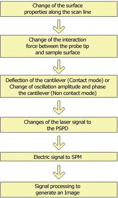
Figure 2. Schematic diagram of the surface property measurement by the advanced Park AFM modes.
Almost every surface property measured by AFM is acquired by the process depicted in Figure 2. EFM measurements follow the same procedure. For EFM, the sample surface properties would be electrical properties and the interaction force will be the electrostatic force between the biased tip and sample. However, in addition to the electrostatic force, the van der Waals forces between the tip and the sample surface are always present. The magnitude of these van der Waals forces change according to the tip-sample distance, and are therefore used to measure the surface topography.
Standard EFM
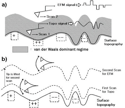
Figure 3. The schematics of (a) Force Range technique and (b) two pass technique.
The standard EFM mode with Park AFM is based on two facts. One is that van der Waals forces and electrostatic forces have different dominant regimes. Van der Waals forces are proportional to 1/r6 while electrostatic forces are proportional to 1/r2. Thus, when the tip is close to the sample, van der Waals forces are dominant. As the tip is moved away from the sample, the van der Waals forces rapidly decrease and the electrostatic forces become dominant. The other fact is that the topography line is the line of the constant tip-sample distance, which equals the line of the constant van der Waals forces.
In the Force Range technique, the first scan is performed by scanning the tip in the region where the van der Waals forces are dominant for topography imaging. Then, the tip-sample distance is shifted to place the tip in the region where the electrostatic force is dominant and an EFM image is scanned as shown in Figure 3 (a).
In the Two-Pass technique, the first scan is performed to obtain the topography by scanning the tip near the sample surface, as done in Non-Contact mode, in the region where the van der Waals forces are dominant. In the second scan, system lifts the tip and increases the tip-sample distance in order to place the tip in the region where electrostatic forces are dominant. The tip is then biased and scanned without feedback, parallel to the topography line obtained from the first scan as shown in Figure 3 (b), therefore maintaining constant tip-sample distance.
Since the topography line is the line of constant van der Waals forces, the van der Waals forces applied to the tip during the second scan are constant. Thus, the only source of the signal change will be the change of the electrostatic force. So, from the second scan a topography free EFM signal can be obtained.
Enhanced EFM
Three extra EFM modes are supported by Enhanced EFM for Park AFM. They are Dynamic Contact Electrostatic Force Microscopy (DC-EFM), Piezoelectric Force Microscopy (PFM), and Kelvin Probe Force Microscopy (KPFM). DC-EFM, patented by Park Systems under US Patent 6,185,991, and PFM are largely identical techniques. KPFM is also known as Surface Potential Microscopy.
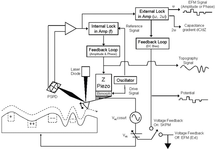
Figure 4. Schematic diagram of enhanced EFM of the Park AFM series.
The unique EFM capabilities are patented and provided only by Park Systems.
The schematic diagram of Enhanced EFM for Park AFM is shown in Figure 4. An external lock-in amplifier is connected to the Park AFM for two purposes. One is to apply an AC bias of frequency (ω) to the tip in addition to the DC bias being applied by the Park AFM controller. The other purpose is to separate the frequency (ω) component from the output signal. This unique capability offered only through the Enhanced EFM is what distinguishes it from the standard EFM hardware for Park AFM.
In Enhanced EFM, the voltage between the tip and the sample can be expressed by the following equation (1):
VDC is the DC offset potential, VS is the surface potential on the sample, and VAC and ω are the amplitude and frequency of the applied AC voltage signal, respectively.
The electrostatic force applied to the cantilever can be expressed by Equation (2), which uses the parallel plate capacitor model to describe the electrostatic interaction between the cantilever and the sample. Here, F is an electrostatic force applied to the tip, q is the charge, E is the electric field, V is the electric potential difference, C is the capacitance, and d is the tip-sample distance. Note that since both AC and DC bias are applied between the tip and the sample, three terms arise in the expression for the force between the tip and the sample. These terms can be referred to as the DC term (a), the ω term (b), and the 2ω term (c). The total cantilever deflection signal, which represents the force between the tip and sample, can be analyzed in terms of its separate parts: DC part, AC part with a frequency of ω, and AC part with a frequency of 2ω.
The DC cantilever deflection signal can be read directly from the signal channels accessible using the XEP Data Acquisition software. The AC parts of the cantilever deflection signal can be read by sending the signal to a lock-in amplifier, which can read either the part of the signal with a frequency of ω or the part of the signal with a frequency of 2ω. Together, the three signals can be used to gain information about the electrical properties of the sample. For example, the capacitance appears in the equation as the ratio of capacitance to tip-to-sample spacing, C/d. If the tip-to-sample distance is kept constant by the Z-feedback loop, then C/d is proportional to the capacitance. The ω signal, which is the coefficient of the term labeled (b) in equation (2) above, contains contributions from both C/d and the surface potential, Vs. Assuming VDC and VAC are known, you still cannot separate the contributions of the capacitance and the surface potential to the measured ω signal. However, the 2ω signal, which is the coefficient of the term labeled (c) above, only includes a contribution from the capacitance. Thus, the 2ω signal can be used to normalize the ω signal, isolating the contribution of the surface potential.
Images can be generated from any of the above-mentioned signals. Analysis of an image involves understanding each of the contributions to the signal used to generate the image.
EFM (one-pass) Mode
EFM (one-pass) Mode is an Enhanced EFM technique that operates in Non-Contact mode while using an external lock-in amplifier. In the EFM (one-pass) Mode, the tip scans over the surface while oscillating in frequency f to obtain a non-contact AFM topography image. At the same time, an AC bias of frequency ω is applied to the tip via an external lock-in amplifier and a DC bias is applied from the control electronics. This design is especially advantageous if a user wishes to use a third-party external lock-in amplifier with greater capabilities than the lock-in amplifier available from Park Systems. This results in an electrostatic force between the AC biased tip and charged surface. Using the external lock-in amplifier, the signal resulting from the tip's motion due to the force can be decomposed and analyzed into a DC part, frequency ω part, and frequency 2ω part. The ω part of the signal contains information on the surface charge, and the 2ω part of the signal contains information about the surface capacitance gradient between the tip and the sample (dC/dz). The frequency ω is chosen to be smaller than the cantilever oscillation frequency f, so that the two signals do not interfere with each other.
The key advantages of Enhanced EFM (one-pass) are as follows:
• Non-invasive True Non-Contact™ AFM
• Small electrical load due to small capacitance
• High spatial resolution
• Ambient operation
• High voltage resolution ( 50 mV ~ 1 mV )
• High measurement bandwidth (DC ~ 100 GHz )
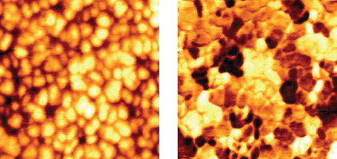
(a) (b)
Figure 5. (a) Topography and (b) EFM phase image of the PZT film by Enhanced EFM (one-pass).