


Probing the Local Electronic Structure of a Sample’s Surface
Although bulk property measurements once provided accurate information for material processing, in recent years, technological advances have placed many demands on materials such that bulk property measurements no longer adequately describe them. This is especially true in the semiconductor, solar, and hard drive industries where device and critical dimensions continue to decrease year after year. In these cases, measuring local properties can help to increase the accuracy of the measurement over bulk property values. Atomic Force Microscopy (AFM) plays a major role in the measurement of local surface properties. Using Conductive AFM, one can simultaneously measure topography and current distribution (conductivity) over the sample surface by using the AFM tip as a nanometer-scale electrical probe.
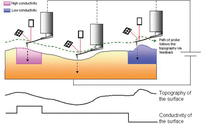
Figure 1. Schematic diagram of the Park AFM series Conductive AFM system
The operation of the Conductive AFM is similar to Scanning Tunneling Microscopy (STM), in which a bias voltage is applied between tip and sample and the tunneling current between the two is measured. The main difference between the two modes is the type of probe used. STM uses a sharpened metallic wire/tip whereas Conductive AFM uses a conductive cantilever. In Conductive AFM, during imaging, while a conductive cantilever scans the sample surface in contact to produce a topography map, the electric current between the cantilever and the sample is measured simultaneously (Figure 1). While the topography is acquired using the deflection signal of the cantilever, the electric conductivity is measured through an electric current amplifier (Figure 2). Since the electric current through the cantilever can be as small as a pico-ampere, the current amplifier is chosen so that the electrical noise is suppressed on the order of a femto-ampere.
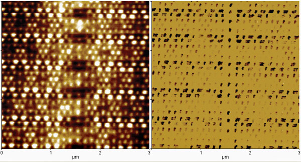
Figure 2. The topography of a DRAM surface (left) and the Conductive AFM image (right) acquired simultaneously. The contrast on the Conductive AFM image indicates differences in the electrical property of the raised dots. (Scan Size: 3 μm × 3 μm )
To achieve the low electric noise level required for Conductive AFM, Park Systems utilizes current amplifiers. Three Conductive AFM sub-modes are available and named according to the current amplifier being used. These submodes are: Internal Conductive AFM, Variable-Enhanced Conductive AFM (VECA), and Ultra Low-Noise Conductive AFM (ULCA). Internal Conductive AFM, which uses an embedded amplifier, measures general samples with a current range up to 10 μA and 1 pA noise level. VECA, with its variable gain setting, is adaptable to wide range of conductivity of up to 10 μA with the noise level of 0.3 pA (Figure 3). ULCA, from its ultra low-noise circuit design, achieves a noise level of less than 0.1 pA, which is effective in observing variations on highly insulating samples.
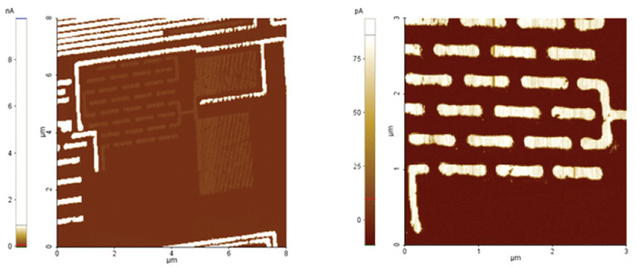
Figure 3. Conductive AFM data of an integrated circuit acquired by the VECA.
The wide dynamic range of VECA enables measurement of both highly conducting and highly insulating areas.
The image on the right is a scanned enlargement of the center portion of the left image.
For detailed investigations of the sample properties, Conductive AFM can be used to measure the IV relationship of a surface. Since the contact size of the AFM cantilever tip can be as small as a few nanometers, the local variation of the electrical property, which is unseen in the macroscopic level, can be observed by the IV curve (Figure 4).
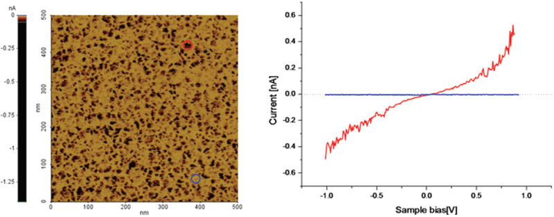
Figure 4. The Conductive AFM data (left) of Nickel Silicide on Silicon Nitride substrate.
Two IV curves (right) are measured on the marked positions in the acquired Conductive AFM image.
Specifications
| Internal Conductive AFM | VECA | ULCA | |
| Maximum Current | 10 μA | 10 mA[2] | 100 pA |
| Gain | Fixed | Variable (103 – 1011 V/A) | Fixed (1011 V/A) |
| Noise level | 1 pA | 0.3 pA[1] | < 0.1 pA |
| Bias range | -10 V – 10 V (0.001 V increment) | ||
| Spatial resolution | Limited by the tip size of the cantilever | ||
| Recommended probe | CDT-CONTR / PPP-CONTSCPt | ||
[1] The noise level of the VECA at the gain of 109 V/A. The noise level may be changed by the gain.
[2] The maximum current range of the VECA at the gain of 103 V/A. The maximum current range decreases according to the gain value.