


-
SiliconOxide SurfaceOxidation MultiLayerCeramicCapacitor Hexylthiophene silicon_oxide Aggregated_molecules Techcomp Stiffness CopperFoil MonoLayer Pinpoint MechanicalProperty Sphere ScanningIon-ConductanceMicroscopy Electical&Electronics Gallium_Arsenide UnivCollegeLondon SPMLabs Regensburg PS_PVAC vertical_PFM TemperatureControl #Materials Composition GlassTemp Chemical Vapor Deposition BiasMode Polyaniline Biology Co/Cr/Pt SoftSample nanomechanical FailureAnalysis Yeditepe_University NCM\
Report image
If you found this image unacceptable, please let us know. We will review your report and take action if we determine this image is really unacceptable.
Atomic steps on GaP(Gallium Phosphide) layer on Si
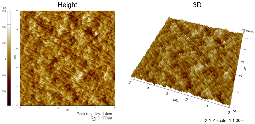
Scanning Conditions
- System: NX20
- Scan Mode: Non-contact
- Cantilever: PPP-NCHR (k=42N/m, f=300kHz)
- Scan Size: 5μm×5μm
- Scan Rate: 1Hz
- Pixel: 512×512