


-
HACrystal organic_polymer OxideLayer Resistance dichalcogenide NiFe Chemical Vapor Deposition Permalloy BiasMode suspended_graphene amplitude_modulation medical FailureAnalysis UnivCollegeLondon Edwin ito_film single_layer graphene_hybrid InLiquid Dimethicone Pipette NanoLithography PtfeMembrane STM PyroelectricDetector SKKU UnivOfMaryland Oxidation HardDiskMedia Cross-section Litho conductive Mechanical InorganicCompound sputter
Report image
If you found this image unacceptable, please let us know. We will review your report and take action if we determine this image is really unacceptable.
BN thin film on Si
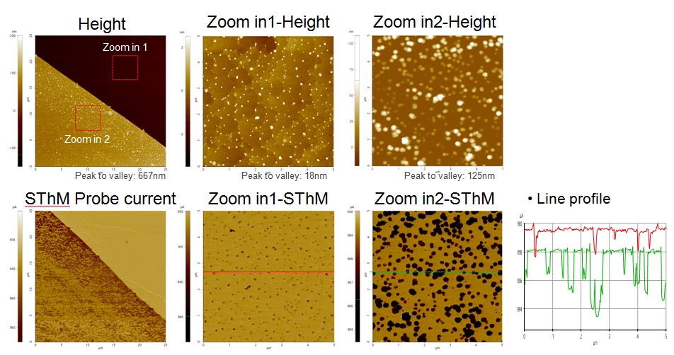
Scanning Conditions
- System: NX10
- Scan Mode:SThM
- Cantilever: Nanothermal probe
- Scan Size: 25μm×25μm, 5μm×5μm
- Scan Rate:0.3Hz, 0.5Hz
- Pixel: 256×256, 256×256
- Scan Mode:SThM
- Cantilever: Nanothermal probe
- Scan Size: 25μm×25μm, 5μm×5μm
- Scan Rate:0.3Hz, 0.5Hz
- Pixel: 256×256, 256×256