


-
Boron fe_nd_b PolymerPatterns OpticalModulator FloppyDisk WWafer margarine Memory rubber SelfAssembly Scratch Pores SiliconOxide CompactDisk StyreneBeads Defect Barium_titanate Phase AM-KPFM Litho GaP HexacontaneFilm OpticalWaveguides PinPointMode Mfm molecular_beam Force-distance P3HT University_of_Regensburg conductive PFM Adhesive Chungnam_National_University PrCurve TPU
Report image
If you found this image unacceptable, please let us know. We will review your report and take action if we determine this image is really unacceptable.
Trench Etch Profile on Si Wafer
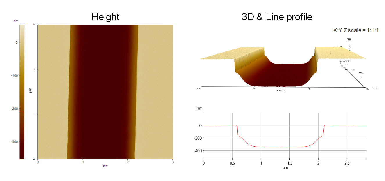
Top dielectric trench etch profile on Si wafer having tapered slope at the trench sidewall.
Scanning Conditions
- System: NX20
- Scan Mode: Non-contact
- Cantilever: AC160TS (k=26N/m, f=300kHz)
- Scan Size: 3μm×3μm
- Scan Rate: 0.21Hz
- Pixel: 1024 × 256
- Scan Mode: Non-contact
- Cantilever: AC160TS (k=26N/m, f=300kHz)
- Scan Size: 3μm×3μm
- Scan Rate: 0.21Hz
- Pixel: 1024 × 256