


-
Nanopattern SKPM HBN Conduct Spain PhaseTransition Filter MechanicalProperties temperature_control pulsed_laser_deposition Metal FrictionalForceMicroscopy HydroGel dielectric trench Treatment Protein Titanate Chungnam_National_University Non-ContactMode Zhi Dopped Phosphide SRAM DataStorage Co/Cr/Pt Butterfly WS2 molecular_self_assembly PolyvinylAcetate Electrical&Electronics ItoGlass ULCA Cobalt tip_bias_mode LiftHeight
Report image
If you found this image unacceptable, please let us know. We will review your report and take action if we determine this image is really unacceptable.
Taegeuk Mark Lithography on PZT
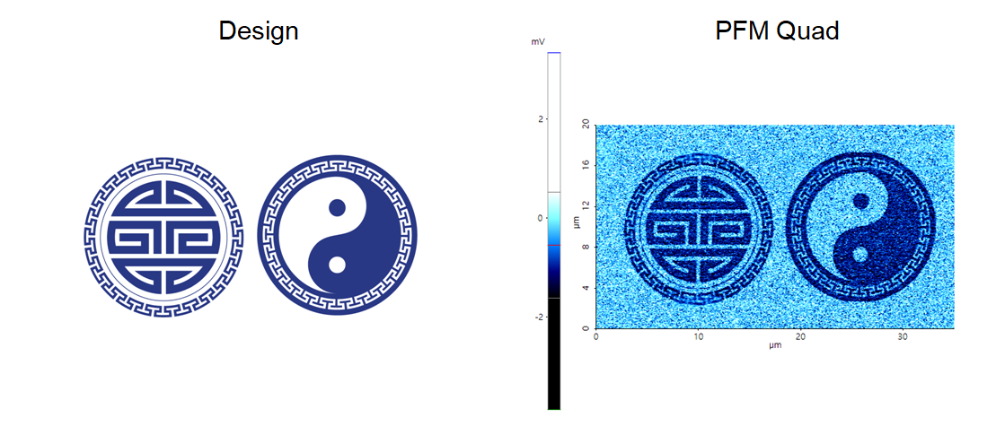
Re-arranged the domain pole direction on PZT surface using bias mode of lithography.
Scanning Conditions
- System: NX10
- Scan Mode: Lithography
- Cantilever: PPP-ContScPt (k=0.2N/m, f=25kHz)
- Scan Size: 35μm×20μm
- Scan Rate: 0.5Hz
- Pixel Size: 1024 × 1024
- Tip Bias: 10V for patterned area
- Scan Mode: Lithography
- Cantilever: PPP-ContScPt (k=0.2N/m, f=25kHz)
- Scan Size: 35μm×20μm
- Scan Rate: 0.5Hz
- Pixel Size: 1024 × 1024
- Tip Bias: 10V for patterned area