


-
CntFilm PvdfFilm Calcite Nanostructure norganic PVAC H-BN OpticalWaveguide MoS2 Lanthanum_aluminate 2dMaterials DeflectionOptics Ananth Hafnia CalciumHydroxyapatite Fet TappingMode ElectrostaticForceMicroscopy Mechinical Aluminium_Oxide blended polymers Sadowski Floppy Implant cooling OpticalModulator MeltingPoint MBE PDMS Liquid Vinylpyridine PpLdpe TemperatureControlledAFM Copper Forevision
Report image
If you found this image unacceptable, please let us know. We will review your report and take action if we determine this image is really unacceptable.
Monolayer Graphene on PDMS Surface
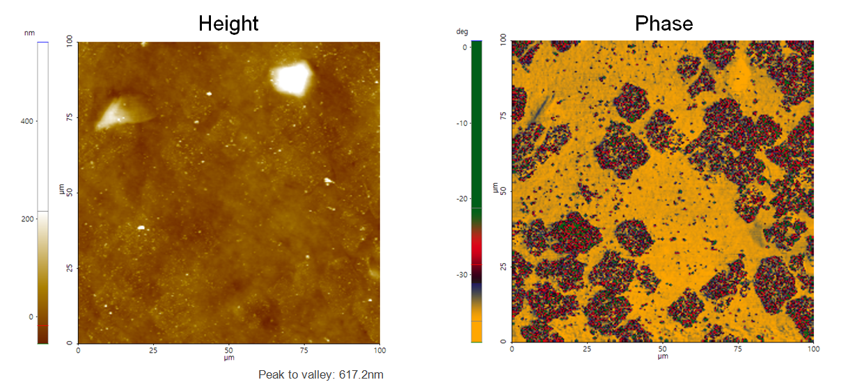
Monolayer Graphene grown on Cu foil using CVD process is transferred on to PDMS substrate.
Scanning Conditions
- System: NX20
- Scan Mode: Tapping
- Cantilever: Access-NC (k=113N/m, f=330kHz)
- Scan Size: 100μm×100μm
- Scan Rate: 0.6Hz
- Pixel Size: 256 × 256
- Scan Mode: Tapping
- Cantilever: Access-NC (k=113N/m, f=330kHz)
- Scan Size: 100μm×100μm
- Scan Rate: 0.6Hz
- Pixel Size: 256 × 256