


-
Platinum Thermoplastic_polyurethane STM CuFoil PvdfBead HACrystal HexacontaneFilm Temasek_Lab hard_disk_media TriGlycineSulphate Melt BFO ScanningThermalMicroscopy InsulatorFilm Conductivity KAIST Kevlar ConductingPolymer Polytetrafluoroethylene HardDiskMedia fluorocarbon Conductive AFM NtuEee Wonseok Alloy SSRM PDMS Tape ForceVolume cross section hard_disk Transparent Imprint Gold Pzt
Report image
If you found this image unacceptable, please let us know. We will review your report and take action if we determine this image is really unacceptable.
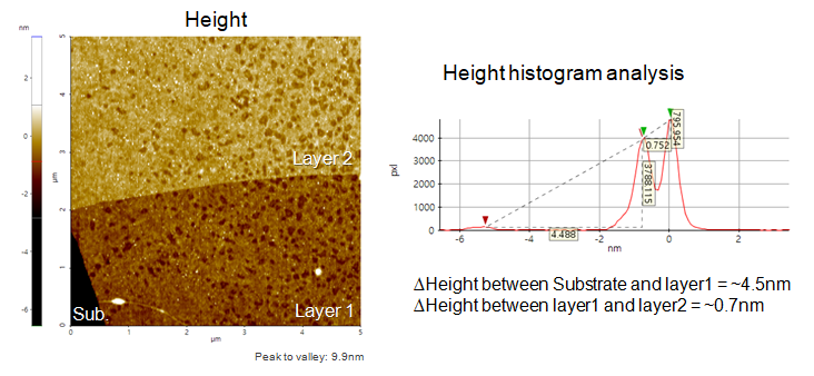
MoS2 Layers on SiO2
Scanning Conditions
- System: NX10
- Scan Mode: Non-contact
- Cantilever: AC160TS (k=26N/m, f=300kHz)
- Scan Size: 5μm×5μm
- Scan Rate: 1Hz
- Pixel Size: 256 × 256
- Scan Mode: Non-contact
- Cantilever: AC160TS (k=26N/m, f=300kHz)
- Scan Size: 5μm×5μm
- Scan Rate: 1Hz
- Pixel Size: 256 × 256