


-
MagneticForceMicroscopy Pore Copper Yttria_stabilized_Zirconia CNT Mosfet Zagreb Chromium Hexacontane tip_bias_mode thermoplastic_elastomers Nanotechnology KAIST NCM semifluorinated_alkane polyvinyl acetate Temperature IIT-chennai 2-vinylpyridine Vanadate Nickel Ferrite MechanicalProperty FrictionalForceMicroscopy Etch UTEM LiquidCell Hafnia Moire ContactMode DLaTGS Electronics HardDisk LightEmiting gallium_nitride
Report image
If you found this image unacceptable, please let us know. We will review your report and take action if we determine this image is really unacceptable.
MoS2 Layers on SiO2
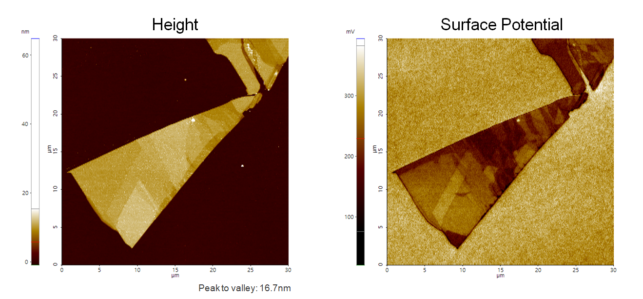
A few layers of MoS2 on SiO2
Scanning Conditions
- System: NX10
- Scan Mode: AM-KPFM
- Cantilever: NSC36Cr-Au B (k=2N/m, f=130kHz)
- Scan Size: 30μm×30μm
- Scan Rate: 0.3Hz
- Pixel Size: 512 × 256
- Scan Mode: AM-KPFM
- Cantilever: NSC36Cr-Au B (k=2N/m, f=130kHz)
- Scan Size: 30μm×30μm
- Scan Rate: 0.3Hz
- Pixel Size: 512 × 256