


Piezoelectric Force Microscopy (PFM) is a scanning probe microscopy technique that utilizes the piezoelectric effect of materials to generate contrast. Performing PFM measurements is enabled through the use of the Enhanced EFM option on a Park AFM.
Basic Principles of PFM
From the day that atomic force microscopy (AFM) was introduced to the contemporary research frontier, new modes and applications have emerged with unprecedented speed, allowing this versatile tool to look into ever-increasing aspects of local material properties at nanometer scale. PFM is one such novel mode which has gained increasing recognition for the unique information it can offer on the electromechanical coupling characteristics of various ferroelectric, piezoelectric, polymer and biological materials.
In PFM, a conductive AFM tip is brought into contact with the surface of the studied ferroelectric or piezoelectric materials, and a pre-set voltage is applied between the sample surface and the AFM tip, establishing an external electric field within the sample. Due to the electrostriction, or "inversed piezoelectric" effects of such ferroelectric or piezoelectric materials, the sample would locally expand or contract according to the electric field. For example, if the initial polarization of the electrical domain of the measured sample is perpendicular to the sample surface, and parallel to the applied electric field, the domains would experience a vertical expansion. Since the AFM tip is in contact with the sample surface, such domain expansion would bend the AFM cantilever upwards, and result in an increased deflection compared to the status before applying the electric field. Conversely, if the initial domain polarization is anti-parallel to the applied electric field, the domain would contract and in turn result in a decreased cantilever deflection (Figure 1). The amount of cantilever deflection change, in such situation, is directly related to the amount of expansion or contraction of the sample electric domains, and hence proportional to the applied electric field.
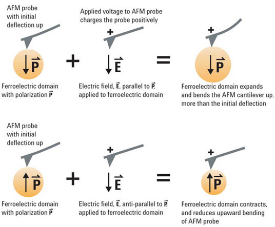 Figure 1
If the applied voltage contains a small AC component, the inversed piezoelectric response from the sample would result in sample surface oscillation in the same frequency as the applied AC voltage. In the case that the sample is an ideal piezoelectric crystal, its polarization would be related to applied mechanical stress by the following equation:
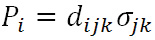
Here, dijk is the rank-3 piezoelectric tensor of the material. For such materials with tetragonal crystal structures, this piezoelectric tensor can be reduced to the following form:
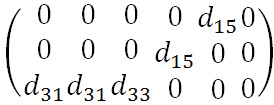
Here, under the applied AC modulation voltage V=V0 cos(ωt), sample surface vibration would take the form ΔZ=ΔZ0 cos(ωt+φ), with the vibration amplitude ΔZ0=d33V0, and phase φ=0 if the sample domain polarization is oriented parallel to the applied electric field, and out of φ=180° if it is oriented anti-parallel to the applied electric field (Figure 2). Such oscillation would be directly reflected in the amplitude and phase signal of the AFM probe contacting the surface, and can be read out using a lock-in amplifier.
 Figure 2
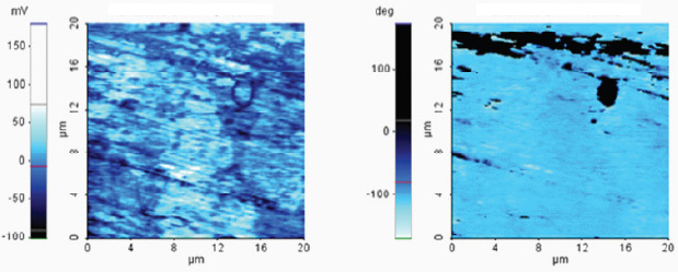
Figure 3
In typical PFM imaging, the applied AC voltage is set to be much lower than the coercive bias for sample domain switching, to avoid alternation of the local domain structure of the studied sample. If such criterion is met, the phase contrast generated in PFM imaging would reflect the domain polarity in different sample locations, while from the magnitude of the amplitude signal local piezoelectric coefficient of the sample can be extracted, as discussed in the former paragraph. Figure 3 shows such an example of such PFM amplitude and phase images obtained on a PZT-5H sample. As can be observed in the circled portion, 180° phase contrast is evident in two adjacent domains in the PFM phase image, and the domain wall between them can be observed with reduced amplitude in the PFM amplitude image. Also, the upward and downward oriented domains have induced a PFM amplitude signal with similar magnitude, indicating the material property is relatively homogenous in the studied sample.
For a more complicated sample domain orientation containing not only components perpendicular to the surface in contact with the AFM tip, but also components along different directions within the surface plane, vector PFM with one vertical and two lateral channels can provide more complete information. For example, to obtain the d15 component of the piezoelectric tensor in tetragonal piezoelectric crystals, we need to measure lateral components of AFM tip vibration proportional to the in-plane sample surface displacement (Figure 4), which would take the form ΔL=ΔL0 cos(ωt+φ), with the vibration amplitude ΔL0=d15V0 Notice if a DC bias is applied between the tip and the sample in conjunction with the AC voltage, both the in-plane and out-of-plane electromechanical response of the sample are also functions of this applied DC voltage.
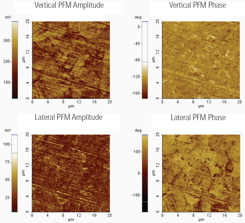
Figure 4
In most of the real cases, the studied sample contains random-oriented polycrystalline grain structure, often with non-zero lateral components in its piezoelectric tensor. In this case, the detected vertical PFM signal is no longer only proportional to d33, but also dependent on the d31 and d15 components. e.g., the vertical PFM amplitude would no longer be ΔZ0=d33V0; instead, it would take the form:
ΔZ0=dzzV0=[(d31+d15) sin2 θcosθ+d33 cos3θ]V0
in which θ is part of the local orientation map (θ,ϕ,ψ) between the lab coordinate system and the crystal coordinate system of the sample. Nevertheless, if both the vertical and two lateral components of PFM signal are obtained on the sample location, either the intrinsic sample piezoelectric constants dij or the local orientation map (θ,ϕ,ψ) can be extracted from such data. In a word, 3D PFM has opened the possibility of a complete 3D reconstruction of the polarization vector of the studied sample at nanometer scale.
Common application of PFM includes local characterization of electromechanical properties of materials, including detailed domain map ping and study of domain switching dynamics; testing of micro- and nano-electromechanical devices (e.g., piezoelectric actuators, transducers, and MEMS), electro-optical devices and nonvolatile memory components (i.e., FERAM devices), addressing their reliability issues such as electromechanical imprint, fatigue and dielectric break-down; exploring the local and global relationship between polarity and other material properties on novel polymer and bio-engineered materials based on detailed nanoscale structural and electrical characterization of such materials, etc.