Park Systems Accurion SIMON imaging ellipsometer combines microscopy and ellipsometry for fast, precise thickness and refractive index measurements, ideal for routine tasks and defect inspection.

Accurion SIMON

Your Entry to Imaging Ellipsometry

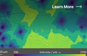
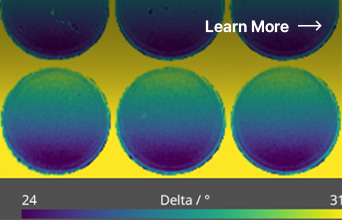
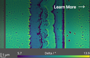
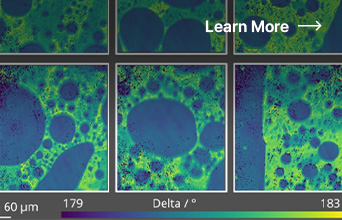
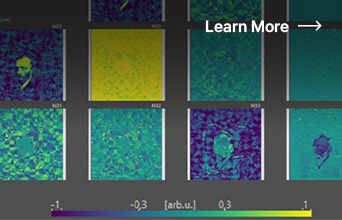
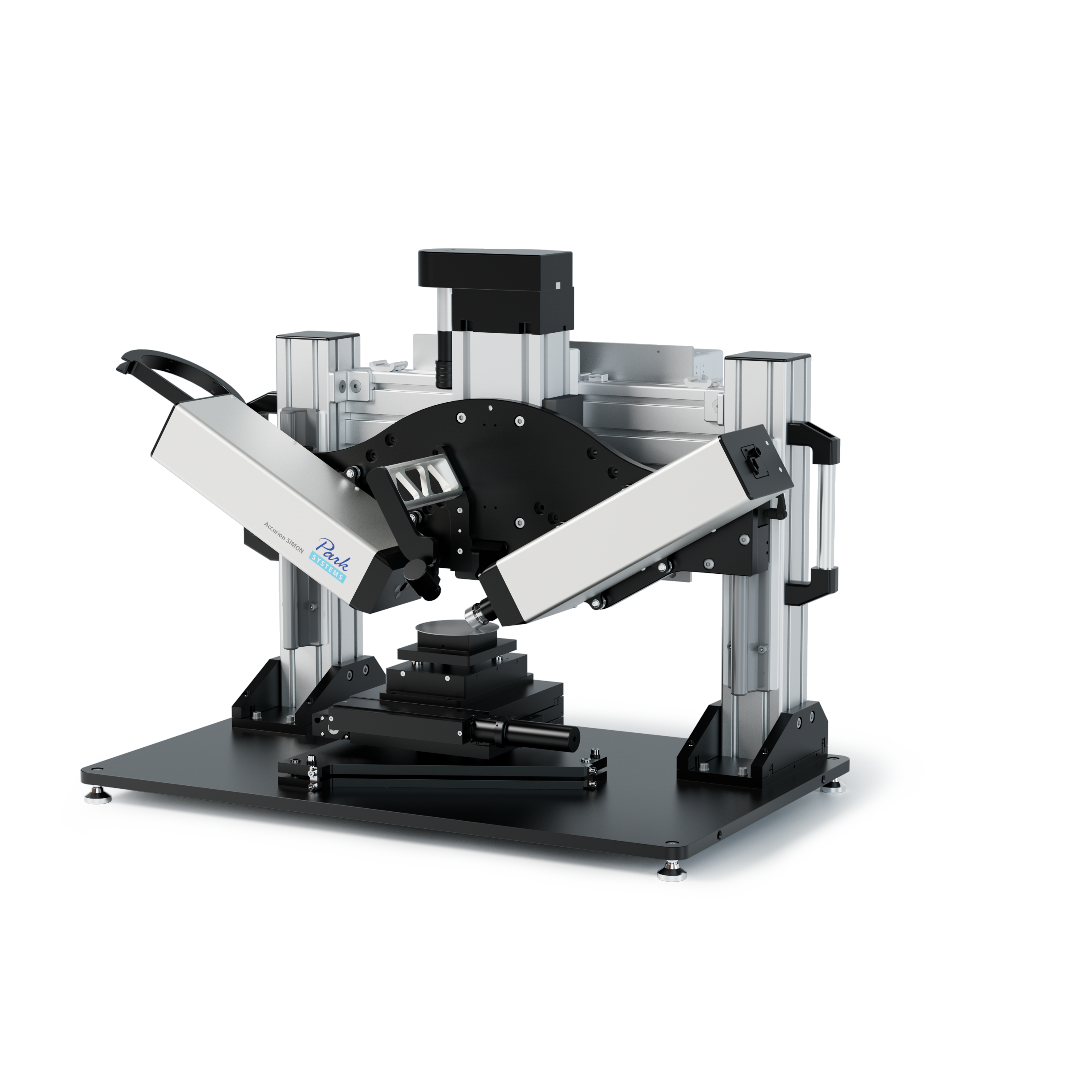
Accurion SIMON is a compact entry-level system for Imaging Ellipsometry, specifically designed for routine measurement and inspection tasks.Based on a fixed-angle ellipsometer design, SIMON offers robust operation and straightforward handling, making imaging ellipsometry accessible for quality control and standard laboratory applications.The system can be operated in two modes:In microscopic mode, rapid visualization of thickness variations and defects is achieved, even for ultra-thin layers such as monolayers (~0.35 nm).In ellipsometric mode, film thickness and refractive index are determined quantitatively.Typical applications include surface inspection of homogeneity and defects on large samples as well as the fast localization of 2D material flakes.

Surface Inspection Metrology of Nanofilms

Typical Applications: Large Area Inspection and Automatic Flake Search

Accurion SIMON enables fast large-area inspection with automated stitching, microscopic defect visualization, and automatic flake detection including histogram-based thickness analysis for efficient quality control.

Thickness and Refractive Index Measurements of Microstructures

Accurion SIMON combines ellipsometry and microscopy to map thickness and refractive index of microstructures with high precision, making even small variations in films and waveguides directly visible.

Key Features

  • Easy-to-use entry-level system for Imaging Ellipsometry, designed for routine inspection tasks
  • Imaging ellipsometry with lateral resolution down to 1 µm for micro-structured samples
  • Quantitative measurement of film thickness and refractive index in ellipsometric mode
  • Fast visualization of thickness distributions and hidden defects across large sample areas
Accurion SIMON Imaging Ellipsometer for fast thickness and refractive index measurement, surface inspection, and automatic flake search on large samples.

Applications

2D-Materials

2D-Materials

Imaging spectroscopic ellipsometry characterizes graphene and other 2D materials, analyzing CVD grown, exfoliated, and epitaxially grown flakes with the ep4 ellipsometer.

Curved Surfaces

Curved Surfaces

Ellipsometry measures thin films and AR coatings on flat and curved surfaces. The ep4 ellipsometer addresses AR coating issues on micro-lens arrays.

Transparent Substrate

Transparent Substrate

Thin films on transparent substrates are key for flexible displays. Knife edge illumination suppresses reflections, allowing non-destructive examination.

Surface Engineering

Surface Engineering

Silanization bonds mineral/inorganic and organic components in paints and adhesives. Imaging ellipsometry examines bond formation in structured arrays without fluorescence markers.

Air-Water Interface

Air-Water Interface

The air/water interface is crucial in biophysics and industry. Brewster angle microscopy (BAM) visualizes Langmuir-Blodgett monolayers and biological materials, investigating molecules, proteins, drugs, DNA, and nanoparticles.

Anisotropic Films

Anisotropic Films

Anisotropic micro crystals are promising for electronics. Imaging Mueller Matrix Ellipsometry (IMME) measures refractive indices and optical axis orientation in anisotropic thin-film samples like Black Phosphorous.

Bio Interfaces

Bio Interfaces

Imaging Ellipsometry (IE) provides high sensitivity for mono- and sub-monolayer thickness. It offers micromaps of ellipsometric angles and a contrast mode for thickness changes. Accessories like cells and QCM-D enhance its biological application capabilities.

MEMS

MEMS

Spectroscopic ellipsometry measures MEMS structures as small as 1µm, with 0.1nm film thickness resolution. A single measurement provides thickness, refractive index, composition, and contaminations. ECM mode allows fast quality control and curved surface measurements.

Photonics

Photonics

Spectroscopic ellipsometry measures optical fibers and waveguides with 1µm lateral resolution and 0.1nm thickness resolution. It covers 190nm to 1700nm, providing optical data and fast quality control.

Displays

Displays

Spectroscopic measurements on micron-scale regions use the ROI concept for multiple measurements in one run. The UV range down to 190nm characterizes display materials. A single measurement provides thickness, dispersions, and compositions, with RCE6 mode allowing sub-20-second tact times.

Battery Materials

Battery Materials

Operando Imaging Ellipsometry monitors battery electrode materials during charging and discharging, measuring microscopic maps of Delta and Psi. It provides data from various regions, with post-processing analysis including profiles, sub-region, and histogram analysis.