


纳米在线课程 原子力显微镜的专家们提供线上在线课堂教学方式, 足不出户也可以免费听取AFM课程:课程包括网络讲座,Live Demos, AFM相关教育视频,软件运作和纳米科学论坛等视频!
近期网络讲座
PinPointing Polymers: Nanomechanical Characterization of Functional Polymer Blends
3 December, 2020
In this webinar, we will describe and demonstrate polymer characterization using PinPointTM mapping on Park System’s NX10 atomic force microscope. Additionally, we will demonstrate example measurements where electrical property maps are acquired simultaneously with topography and nanomechanical maps.
Nailing down Teflon Molecules : High Resolution AFM imaging for Polymer Science
12 November, 2020
In this webinar, we will demonstrate how atomic force microscopy (AFM) can be used to acquire ultra-high-resolution images of individual PTFE-molecules on the semi-crystalline surface of commercial Teflon tape. Both high resolution and high-speed scanning capabilities of Park Systems NX20 AFM will be demonstrated on the real-world polymer sample.
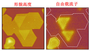
二维材料界面结构与性质的原子力探针显微学研究(2)- 力学结构与性质
2020年11月5日*星期四 北京时间东八区上午11:00-12:00
本系列报告,将基于我们在原子力显微术的技术研究工作,利用多种先进原子力显微术针对二维材料的本征界面、异质界面以及材料/基底界面开展的研究工作。在每次报告中,我们首先将在较为详细地介绍主要使用的先进AFM模式的基本原理、技术实现及其相关应用。在此基础上,介绍我们利用该AFM模式所开展的关于二维材料界面结构与性质方面的研究工作。希望通过本系列报告有助于相关AFM使用者能够利用比较复杂的AFM功能模式开展研究工作。
Nano: High Resolution AFM imaging for Polymer Science (Joint webinar with Nano Nature)
10am and 5pm, 28 October, 2020
In this webinar hosted by Nano Nature, guest presenter Dr. Vladimir Korolkov (Senior Application Scientist at Park Systems UK) will demonstrate how to better understand the overall structure of polymers. You will learn to resolve individual polymer chains in real space, and witness how atomic force microscopy (AFM) can be used to acquire ultra-high-resolution images of individual PTFE-molecules on the semi-crystalline surface of commercial Teflon tape.
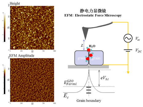
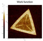
利用静电力显微镜研究ZnO薄膜的耐湿热稳定性
2020年10月22日*星期四 北京时间东八区上午10:00-11:00
本讲座以多晶ZnO基TCO薄膜的耐湿热稳定性为出发点,结合静电力力显微镜(EFM: Electrical Force microscopy)研究ZnO薄膜的晶界稳定性对耐湿热性能的影响,展示了原子力显微镜在氧化物晶界研究中的巨大潜力。
AFM option mode to monitor sample’s properties (with live demo)
October 20, 2020
In this session, a variety of AFM option mode is introduced for investigating sample’s properties such as electrical, mechanical, magnetic, thermal and electrochemical properties. Based on Contact or Non-contact mode, AFM option mode can be combined to monitor sample’s properties as well as topography. Also, we highlight the applications and representative images at each option mode to help your understanding about AFM option mode.

导电原子力显微镜在电子器件纳米级电学测试中的应用
2020年9月24日*星期四 北京时间东八区上午9点到下午6点
导电原子力显微镜(C-AFM)是在扫描探针显微镜(SPM)基础上扩展的一种电学测试模式,它可以同时实现在纳米级对样品(比如:介质材料、量子点、电子器件)表面形貌和局部电学性质的表征和测试。C-AFM 技术在纳米电子学、半导体材料等领域广泛应用,主要用于表征样品/器件的缺陷分布、电导率局部变化、局部电学行为等。本报告将重点围绕C-AFM在忆阻型电子器件中的电学表征,介绍不同环境(大气和真空状态)下测试结果的可靠性,以及通过使用基于C-AFM技术的不同手段来直接观测导电细丝的形成以进一步探索阻变机理。
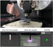
How to operate AFM (with live demo)
Tuesday, 22 September, 2020 / 13:30 pm SGT
In this session, the basic principles and the application of AFM which can be used in scientific and industrial fields are examined. In particular, we share the images measured by the actual atomic force microscope with specific examples of various applications and look at their meaning. In addition, we present how to operate AFM including cantilever selection, sample preparation, description of imaging parameters and operation in order to obtain better understanding for AFM.
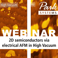
Better in Vacuum – boosting the characterization of 2D semiconductors via electrical AFM in high vacuum
Thursday, 3 September 2020
This webinar explains the basics of EC-AFM and investigation of localized electrochemical deposition and dissolution of copper using the Park NX12 AFM System.
二维材料界面结构与性质的原子力探针显微学研究(1)
2020年8月27日*星期四 北京时间东八区上午11:00-12:00
本系列报告,将基于我们在原子力显微术的技术研究工作,利用多种先进原子力显微术针对二维材料的本征界面、异质界面以及材料/基底界面开展的研究工作。在每次报告中,我们首先将在较为详细地介绍主要使用的先进AFM模式的基本原理、技术实现及其相关应用。在此基础上,介绍我们利用该AFM模式所开展的关于二维材料界面结构与性质方面的研究工作。希望通过本报告有助于相关AFM使用者能够利用比较复杂的AFM功能模式开展研究工作。
网络讲座复播视频
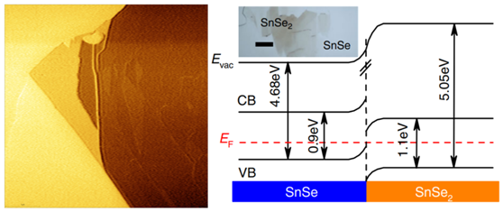
用原子力显微镜研究热电材料中的缺陷物理
原子力显微镜在材料表面形貌和性质的研究中起着重要的作用,不仅可以用于薄膜材料,也可以用于研究单晶表面。热电材料能够利用赛贝克(Seebeck)效应收集废热发电,是一种潜在的绿色能源材料。
原子力显微镜用于体相异质结太阳能电池
原子力显微镜(AFM)是功能强大的扫描探针显微镜(SPM)技术之一,其能将薄膜的局部性质和微区形貌在微米尺度上统一起来,在诸多研究领域得到了广泛的应用。同时,无铅金属卤化物钙钛矿材料,由于其稳定性和对环境无毒性的优点,在LED和太阳能电池方面展现出巨大的研究潜力。
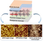
原子力显微镜在钙钛矿太阳能电池中的应用
更多信息请关注公众号:帕克原子力显微镜Park 原子力显微镜(AFM)是功能强大的扫描探针显微镜(SPM)技术之一,其不仅可以探测薄膜的形貌,而且可以表征薄膜的相组成和表面电势。与此同时,钙钛矿太阳能电池近期也引起了人们的广泛兴趣,而钙钛矿薄膜的形态和质量对器件性能有着至关重要的影响。
扫描隧道显微镜(STM)崭新技术和 Park SmartScan
Park原子力显微镜的应用团队很自豪地向您推荐我们的扫描隧道显微镜(STM)模式,这是一种可以在垂直和水平方向实现原子分辨率的表征技术。
教育型网络讲座“AFM技术”
Atomic Force Microscopy PinPoint Nanomechanical Mode for Nanoscale Modulus Mapping – Cantilever Modulus and Applied Force
The applications staff of Park Systems will give this webinar on atomic force microscopy PinPoint Nanomechanical Mode for Nanoscale Modulus Mapping, specifically, we will look at the influence of cantilever stiffness and applied force on the measured modulus.
PinPoint Piezoelectric Force Microscopy
PFM functions by engaging a sample surface with a sharp conductive SPM probe. This probe's tip then has an alternating current (AC) bias applied to it in order to cause a deformation of the sample surface by way of a piezoelectric force.
Electrochemical Atomic Force Microscopy (EC-AFM)
In EC-AFM, users typically perform voltamemetry and corrosion experiments using an electrochemistry cell and a choice of potentiostat or galvanostat depending on the electrochemical application of interest.
PinPoint Nanomechanical Imaging Using Probes of Various Cantilever Stiffness
PinPoint Nanomechanical mode obtains the best of resolution and accuracy for nanomechanical characterization. Stiffness, elastic modulus, adhesion force are acquired simultaneously in real-time.
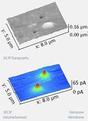
Scanning Ion Conductance Microscopy (SICM) and Scanning Electrochemical Microscopy (SECM)
SICM uses the increase of access resistance in a nanopipette placed in an electrolyte solution and monitors the ionic current flowing in and out of this probe—a flow that is hindered as the tip closes in on a sample surface.
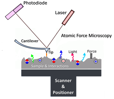
教学视频“原子力显微镜的工作原理”
| Topic | |
|---|---|
| 原子力显微镜的原理 | 扫描离子电导显微镜 |
| 接触模式 | 力-距离分光镜 |
| 非接触模式 | 磁力显微镜 |
| 轻敲模式 | 力调制显微镜 |
| 动态接触式静电力显微镜 | 横向力显微镜 |
| 静电力显微镜 | 纳米压痕 |
| 导电原子力显微镜 | 纳米光刻 |
| 电流-电压分光镜 | 热扫描显微镜 |
| 扫描电容显微镜 | |
| 扫描开尔文探针显微镜 | |